
Yesterday in my micro-nano lab class, we learned how to use a scanning electron microscope (SEM) to take micron-resolution images of samples with interesting surface properties. I’ve only ever seen SEM images in National Geographic and published papers, so this was one of the coolest things I’ve ever done in a lab class.
Because the SEM uses an electron beam rather than visible light to capture images, there’s no color data in these images. However, there wouldn’t be much color to look at anyway: the surface of the object being imaged has to be conductive for the incoming electron beam to scatter properly, so non-conductive objects, like a lotus leaf, must be sputter-coated in a layer of gold or platinum a few nanometers thick before they can go into the SEM. Any existing coloring is covered up by a uniform bronze.
Surprisingly, one of the most brightly-colored samples we had to look at, a piece of a morpho butterfly wing, didn’t need to be sputter-coated. Butterfly wings are actually quite conductive, and they’ve been used as inspiration for more efficient photoanodes in solar cells. That said, the morpho butterfly scales still wouldn’t look colorful up close, because that magnificent blue color is structural coloration, not pigmented coloration — it’s the microstructure of the scales themselves that causes light to scatter and create the beautiful iridescence of the wings.
[NB: I took the beetle images; the butterfly wing and carbon nanotube images were taken by another member of my group.]

A beetle of indeterminate species; I was struck by the unusual joints on the leg.

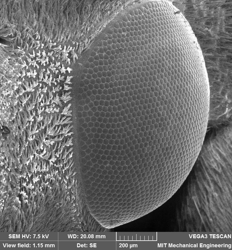
10x close-up of the compound eye from the first image, with a clearer view of individual ommatidia.

A carbon nanotube forest, which we grew in the previous lab session (!)
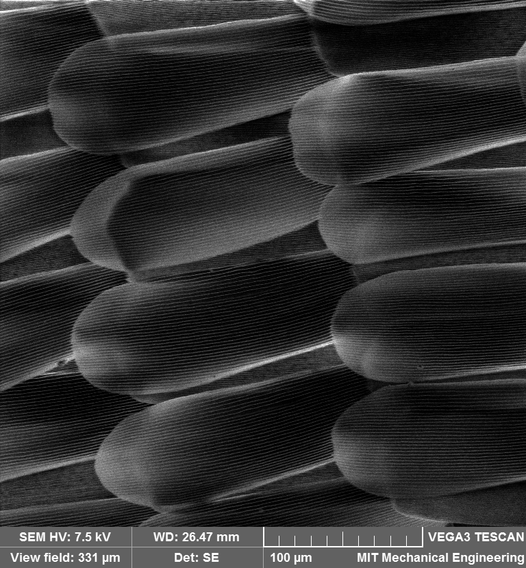
Scales of a morpho butterfly wing.
